Research Achievement
2025
새로운 2차원 전자계 물질의 발견은 연구단의 중요한 연구 주제중 하나이다.특히 특이 격자구조에 의한 평탄밴드가 구현된 물질은 강상관 특성과 위상특성을 동시에 연구할 수 있는 플랫폼이 된다. Nb에 기반한 왜곡된 카코메(breathing Kagome) 반데르발스 물질은 2차원 평탄밴드를 갖는 반데르발스 반도체 물질중 하나로, 그 Nb3TeI7은 카고메 결정 구조 뿐만 아니라 야누스 결정구조로 인해반전대칭성이 깨진 전자상태가 예상되는 물질이다. 고품질 단결정의 투과현미경 실험을 통해 야누스 적층구조를 확인하였고 각도분해 광전자분광 실험을 통해 평탄밴드의 존재와 표면의 화학적 조성에 따른 전자밴드의 휘어짐이 반대가 되는 것도 확인하였다. 이러한 결과는 평탄밴드의 상호작용을 고려한 전자구조 계산을 통해서도 확인되는 데, 이처럼 뚜렷한 반도체 특성과 이중 분극 전자상태가 공존하는 물질이 발견된 것은 이번이 최초이다. 이러한 독특한 특성을 활용해 Nb3TeI7의 박리 단결정 반도체 소자를 제작하고 전계효과에 따른 전도도의 변화를 반대 표면에 대해 관측하여 뚜렷한 n형과 p형 반도체 특성을 확인하였다. 이러한 결과는 반전대칭성 깨진 평탄밴드 전자상태를 구현한 최초의 연구로, 향후 다양한 반도체 또는 스핀 특성 연구로 확장될 것이 기대된다. (Adv. Mater., 37, 9, 2025)
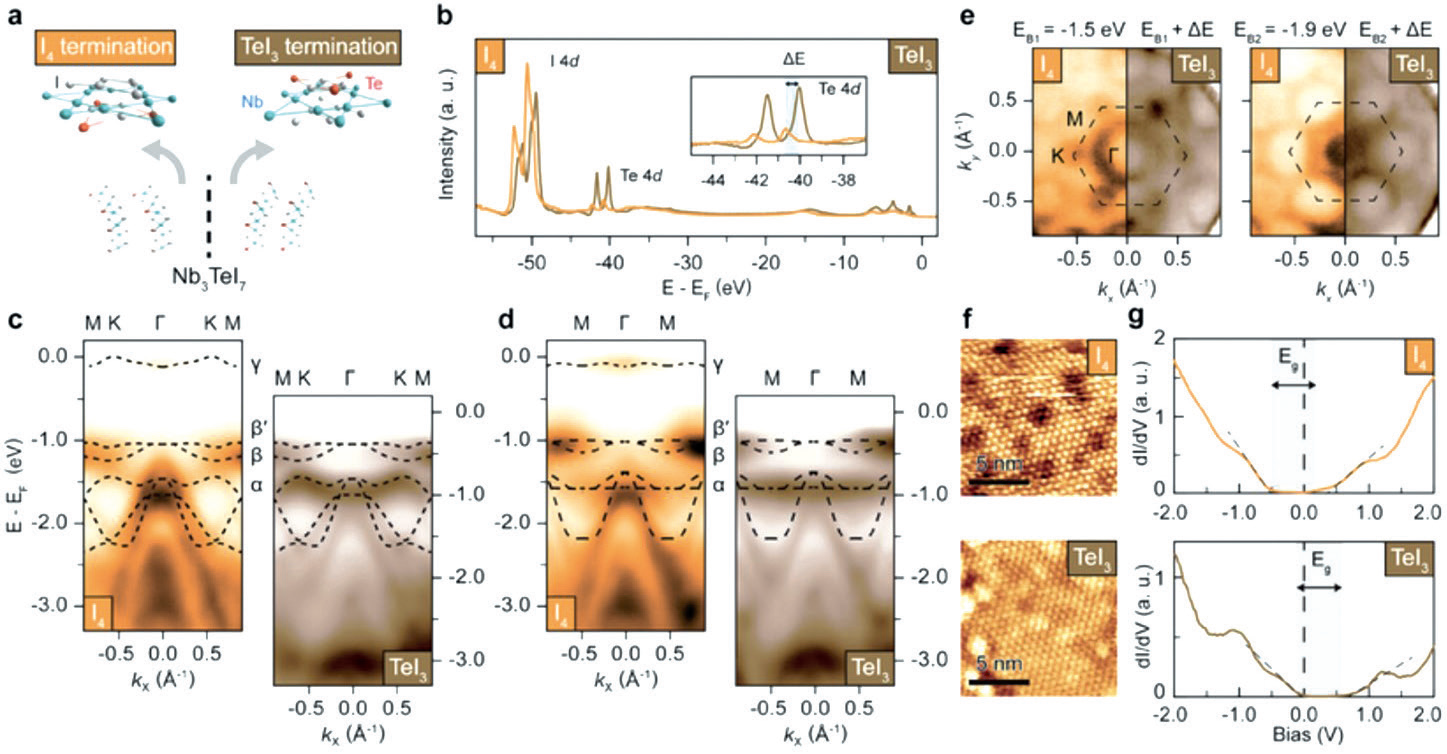
Figure. a, Determination of the surface termination of exfoliated Nb3TeI7 crystals arising from its Janus structure. b, Comparison of the X-ray photoelectron spectroscopy spectra obtained from the TeI3-terminated and I4-terminated surfaces. c,d, Comparison of the electronic structures for the two different surface terminations, confirming a potential difference of approximately 0.7 eV. e, Comparison of the Fermi surfaces at a selected energy plane for the two surface terminations. The same Fermi surface is identified after correcting for the ~0.7 eV energy offset.f,g, Comparison of tunneling spectra measured by scanning tunneling microscopy for the two surface terminations, revealing an approximately 0.7 eV shift in the Fermi level.
The discovery of new two-dimensional electronic materials is one of the major research themes of the center. In particular,materials hosting flat bands arising from unusual lattice structures provide an important platform for investigating both strong correlation effects and topological properties. Nb-based distorted kagome (breathing kagome) van der Waals materials are among the van der Waals semiconductors that exhibit two-dimensional flat bands. Among them, Nb3TeI7 is expected to host inversion-symmetry-broken electronic states owing not only to its kagome crystal structure but also to its Janus crystal structure. Through transmission electron microscopy measurements on high-quality single crystals, we confirmed the Janus stacking structure. Angle-resolved photoemission spectroscopy further revealed the presence of flat bands and showed that the band bending is reversed depending on the surface chemical composition. These results are also supported by electronic structure calculations that take into account interactions associated with the flat bands. To our knowledge, this is the first discovery of a material in which such clear semiconducting behavior coexists with bipolar electronic states. Exploiting these unique properties, we fabricated semiconductor devices based on exfoliated single crystals of Nb3TeI7 and observed opposite field-effect-induced changes in conductivity on the two opposite surfaces, thereby confirming distinct n-type and p-type semiconducting behavior. This work represents the first realization of inversion-symmetry-broken flat-band electronic states and is expected to open new directions for future studies of semiconductor and spin-related properties. (Adv. Mater. 37, 9, 2025).
양자 다체계는 시간의 경과에 따라 다수의 자유도 사이에 양자 얽힘이 생성되며, 이 과정에서 정보가 효과적으로 확산·소실되는 양상을 보인다. 이러한 현상은 양자 카오스로 불리며, 고전역학에서 삼체 이상 계에서 나타나는 카오스의 양자역학적 대응으로 이해된다. 양자 카오스는 자유도 간 정보를 강하게 혼합시키므로, 양자정보 및 양자컴퓨팅에서 활용도가 높은 하 랜덤 상태(Haar random state)를 생성하는 메커니즘으로 알려져 있으나, 양자 카오스를 정밀하게 시뮬레이션하는 것은 막대한 계산 자원을 요구하여 현실적으로 큰 제약이 존재한다.
본 연구진은 이러한 한계를 극복하기 위해, 양자정보 이론의 유사 랜덤 상태 개념과 양자 카오스 개념을 결합한 ‘유사 카오스(pseudochaos)’를 도입하고 이를 구현하는 양자 회로를 설계하였다. 제안된 유사 카오스는 실제 양자 카오스와 실험적으로 구별이 어려운 특성을 가지므로, 양자 카오스의 효율적 시뮬레이션을 가능하게 함과 동시에 (하 랜덤 상태와도 구별이 어려운) 유사 랜덤 상태의 효율적 생성 방법을 제공한다. 이러한 연구는 유사 랜덤 상태를 활용한 양자 시뮬레이션 및 양자 연산에 대한 응용적 가능성을 제시하는 한편, 양자 카오스를 규정하는 물리적지표가 무엇인지에 대한 근본적인 질문을 제기하는 의의를 가진다 할 수 있다. (Nature Communications, 16, 1, 2025)
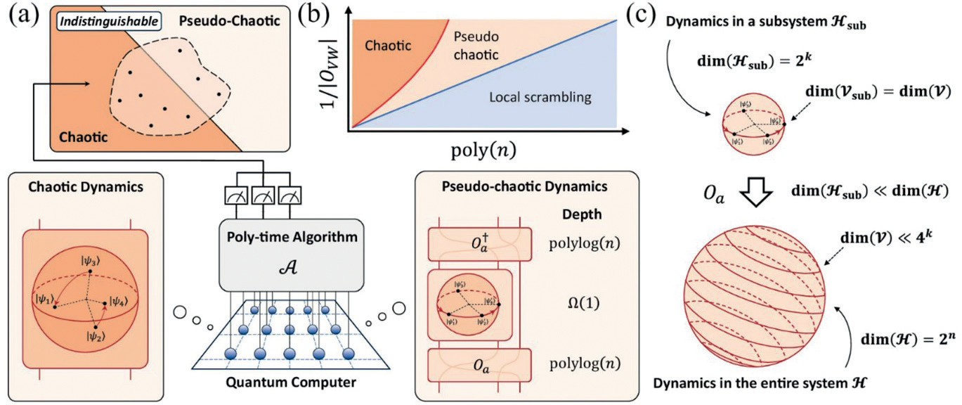
Figure.Comparison between pseudochaos and genuine quantum many-body chaos, and a conceptual illustration of the corresponding quantum circuits. (a) Although pseudochaos and quantum chaos represent distinct forms of quantum dynamics, they exhibit properties that are experimentally difficult (computationally impossible) to distinguish. (b) In particular, even in diagnostics such as the Out-of-Time-Order Correlator (OTOC), where quantitative differences do exist, the two remain effectively indistinguishable in practice. (c) This behavior originates from the fact that pseudochaos and quantum chaos explore parameter spaces with similar underlying structures over time, although the densities with which they sample these spaces may differ.
Quantum many-body systems generate quantum entanglement among a large number of degrees of freedom as time evolves, exhibiting effective spreading and loss of information in the process. This phenomenon is known as quantum many-body chaos and is the quantum-mechanical counterpart of the chaos and butterfly effect that arise in classical systems with three or more interacting bodies. Because quantum many-body chaos strongly mixes information among many degrees of freedom, it can serve as a physical mechanism for generating Haar-random states, which are highly valuable for quantum information processing, quantum computing, and quantum cryptography. However, accurately simulating quantum chaos requires enormous computational resources, posing significant practical limitations.
To overcome these challenges, our research group introduced the concept of “pseudochaos,” which combines the notion of pseudorandom states from quantum information theory with that of quantum many-body chaos, and designed quantum circuits that realize this phenomenon. The proposed pseudochaos exhibits properties that are experimentally difficult to distinguish from genuine quantum many-body chaos, there by enabling efficient simulation of quantum chaos while simultaneously providing an efficient method for generating pseudorandom states that are likewise difficult to distinguish from Haar-random states. This work not only suggests potential applications of pseudorandom states in quantum simulation and quantum computation, but also raises a fundamental question regarding the physical indicators that truly define quantum chaos. (Nature Communications, 16, 1, 2025)
고체물질에서의 엑시톤 기저상태는 1960년대에 이미 이론적으로 가능성이 예측되어 ,Mott 절연체와 함께 대표적인 전자상호작용에 의한 다체적인 절연체상태임에도 불구하고 최근까지 그 존재가 제대로 확인된 바가 없었다. 특히 최근의 연구에서는 반데르발스 반도체와 그래핀의 이중막구조에서 인위적으로 형성되는 경우가 확인되어 많은 연구가 이루어지고 있으나, 고체물질로 자연적으로 존재하는 경우는 2011년 Ta2NiSe5이 제안되었으며, 이후 최근 Ta2Pd3Te5이 보다 확실한 가능성을 보이는 물질로 제시되었다. 이는 본 연구단에서 2021년 Nature Physics에 출판한 논문에서 Ta2NiSe5 결정에서 빛에의해 엑시톤이 해리되어 그 구성 전자가 광전자로 방출되는 양자적인 프로세스, 즉 엑시톤 광전자분광의 특이 신호를 확인함을 보고하였다. 이번 실험에서는 Ta2Pd3Te5에 대하여 동일한 실험을 실시한 결과 Ta2NiSe5의 경우와 거의 동일한 엑시톤 광전자분광 신호를 확인하였는데, 후자의 경우는 엑시톤상전이 온도보다 높은 온도에서만 관찰되었으나, 이번 실험에서는 엑시톤 상전이 온도 이하의 전 온도 범위에서 관찰되었다. 이는 자발적으로 형성된 엑시톤절연체상에서의 엑시톤 광전자분광, 또는 엑시톤 존재자체를 직접 확인한 최초의 성과라 할 수 있다. 이 실험결과는 Ta2Pd3Te5에서의 엑시톤절연체상을 존재를 확실하게 뒷받침하고 있어, 이를 바탕으로 향후 엑시톤절연체의 양자적 성질에 대한 전자물성과 분광학적 연구가 발전할 수 있다 (Physical Review Letters 2025). 아울러 이 물질에 알칼리 금속을 흡착하여, 엑시톤상이 서서히 붕괴되는 과정을 광전자분광으로 측정하여 이를 분석 중에 있다. 또한, 해당 물질의 표면 결함 부근에 발생하는 특이한 전자상태를 주사터널현미경분광으로 확인하였으며 이에 대한 이론적인 해석을 진행중이다.
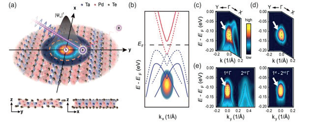
Figure. Schematic diagram of excitonic photoemission in Ta2Pd3Te5 (a). Electronic band structure and distribution of the excitonic photoemission signal of Ta2Pd3Te5d (b).Measurement results of the excitonic photoemission signal of Ta2Pd3Te5d (white arrow) (c).
Excitons are bosonic quasiparticles with a variety of applications in optoelectronics, photosynthesis, and dissipationless informatics, and their lifetime can become sufficiently long to form a quantum condensate.
While exciton condensation has been predicted to occur as a ground state of a solid, so-called an excitonic insulator, whose material realization has been elusive. Here we report the observation of direct photoemission signals from excitons in a ground state of a very recent excitonic insulator candidate Ta2Pd3Te5 below its metal-insulator transition temperature using orbital-selective angle-resolved photoemission spectroscopy. It is confirmed that the excitons have a lower energy than the valence band maximum to possibly drive the phase transition. This measurement further discloses the size and the unusual odd parity of the exciton wave function. The present finding opens an avenue toward applications of coherent excitons in solid systems and searching for exotic quantum phases of exciton condensates.
연구단에서 지속적으로 연구하는 대상인 강한 전자상호작용을 가지는 이차원 Mott 절연체 물질 1T-TaS2의 경우 S를 Se으로 치환하거나, 전자를 도핑하는 경우, 또한 압력을 가하는 경우에 Mott gap이 파괴되어 금속상이 발생이고, 이를 냉각하면 초전도상태가 발생함이 알려져있다. 특히, 이 물질에 고유하게 존재하는 카이럴구조와 카이럴전자구조에 의해, 그리로 초전도의 모태가 Mott 절연체라는 이유에서 통상적인 초전도와 다른 상태를 보일 가능성이 오랜기간동안 연구되어왔다. 본 연구단의 이전 연구에서는 이러한 초전도상을 보이는 TaSSe 원자막의 경우 내부의 S/Se이 무질서한 alloy 상태로 분포하며 이것이 Mott gap을 파괴하고 pseudogap 금속상을 만들어 초전도로 이어진다는 관찰과 해석을 제시한 바 있다. 본 연구에서는 TaSSe을 광전자분광으로 세밀하게 측정하여, pseudogap을 확인하였으며, 이러한 pseudogap이 이 물질에 내재된 chiral 대칭성 붕괴를 반영하여 운동량공간에서 대칭적이지 않은 새로운 형태의 pseudogap이 됨을 밝혔다. 이러한 pseudogap은 chiral pseudogap으로 명명되었으며, 향후 이 새로운 pseudogap이 초전도 현상에 어떤 영향을 끼치게 되는지 밝혀내야 되는 중요한 과제가 남게 되었다 (Advanced Materials 2025)
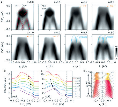
Figure. Changes in the electronic band structure of TaS2-xSEx compound crystals with increasing Se mixing ration (x) (angle-resolved photoemission spectroscopy (ARPES) measurement results, a). A strong pseudogap exists near x=1 (b, c), and it can be observed that the metallic electron density of this pseudogap lacks left-right symmetry in momentum space (d).
The emergence of a pseudogap is a hallmark of anomalous electronic states formed through substantial manybody interaction but the mechanism of the pseudogap formation and its role in related emerging quantum states such as unconventional superconductivity remains largely elusive. Here, the emergence of an unusual pseudogap in a representative van der Waals chiral charge density wave (CDW) materials with strong electron correlation, 1T-TaS2 is reported, through isoelectronic substitute of S. The evolution of electronic band dispersions of 1T-TaS2 – xSex (0 ⩽ x ⩽ 2) is systematically investigated using angle-resolved photoemission spectroscopy (ARPES). The results show that the Se substitution induces a quantum transition from an insulating to a pseudogap metallic phase with the CDW order preserved. Moreover, the asymmetry of the pseudogap spectral function is found, which reflects the chiral nature of CDW structure. The present observation is contrasted with the previous suggestions of a Mott transition driven by band width control or charge transfer. Instead, the pseudogap phase is attributed to a disordered Mott insulator in line with the recent observation of substantial lateral electronic disorder. These findings provide a unique electronic system with chiral pseudogap, where the complex interplay between CDW, chirality, disorder, and electronic correlation may lead to unconventional emergent physics.
기존에 진행하였던 상호작용이 강한 이차원물질인 1T-TaS2의 도메인월 위상여기에 대한 연구를 심화시켰으며, 특히 도메인웰에서 음의 저항 상태(NDR)가 일차원적인 채널의 형태로 발생함을 주사터널현미경 분광으로 발견하였다. 음의 저항 상태는 공명터널다이오드와 같은 비선형특성에 기반한 고주파수 저전력 소자의 핵심적인 작동원리를 제공하여 반도체 물리학과 소자공학에서 오랜 시간 동안 연구되어 오고 있다. 또한 NDR은 나노구조체와, 표면에서의 결함이나 흡착분자 등에서도 발견되어 비선형나노소자 및 분자소자 응용으로 이어지게 된다. 하지만, NDR현상이 일차원적인 채널로 발생하는 경우는 일부 탄소나노튜브에서 보고된 예를 제외하면 거의 보고된 바가 없어, 본 연구에서 발견한 일차원 채널의 NDR 상태는 새로운 형태의 음의 저항을 활용하는 소자로서의 활용이 기대된다 (Advanced Science 2025). 특히, 이번에 발견된 NDR 채널은 1 nm정도의 매우 작은 폭을 가지며 선적인 구조가 잘 정의되고, 특히 두 개의 NDR 채널이 이웃한 형태로 발견되었다. 향후 이러한 성질을 응용한 양자물성과 양자소가 연구로 발전될 수 있다.
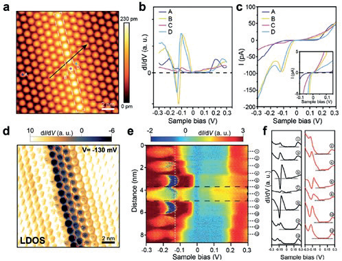
Figure. Domain wall STM image of 1T-TaS2 (a) and STM spectroscopy results showing negative differential resistance (b, c). Spatial distribution of the negative differential resistance (d, e, f).
Negative differential resistance (NDR) is the key feature of resonant tunneling diodes exploited for high-frequency and low-power devices and recent studies have focused on NDR in van der Waals heterostructures and nanoscale materials. Here, strong NDR confined along a 1-nm-wide 1D channel within a van der Waals layer 1T-TaS2 is reported. Using scanning tunneling microscopy, a double 1D NDR channel formed along the sides of a charge–density-wave domain wall of 1T-TaS2 is found. The density functional theory calculation elucidates that the strong local band-bending at the domain wall and the interlayer orbital overlap cooperate to bring about 1D NDR channels. Furthermore, the NDR is well controlled by changing the tunneling junction distance. This result would be important for nanoscale device applications based on strong nonlinear resistance within van der Waals material architectures.
2025년, 본 장비의 본연의 목적인 극한 조건에서의 본격적인 초 고해상도 측정실험에 돌입했다. Td-MoTe2는 반전대칭성이 깨진 비중심대칭(type-II) 바일 반금속으로 위상 초전도 후보물질중 하나이나, 상압에서의 임계온도가 약 100 mK이고 초전도 갭이 수십 마이크로전자볼트 범위에 있어 그 페어링 상태를 직접 규명하기 어렵다. 본 연구에서는 희석 냉동기 기반 분광 이미징 주사 터널링 현미경법을 이용하여 비도핑 Td-MoTe2의 고유한 초전도 갭을 처음으로 관측하고, 그 온도 및 자기장에 따른 변화를 추적하였다. 측정된 스펙트럼은 약 58 μeV크기의 V자형 갭을 보여주었으며 이는 현재까지 보고된 벌크 초전도 갭 중 가장 작은 값으로 보인다. 온도에 대해 거의 선형적인 제로바이어스 전도도, 자기장에 의해 빠르게 증가하는 저에너지 스펙트럼 가중치, 그리고 정확히 0 meV에서 분산이 교차하는 입자-정공 대칭의 갭 내 준입자 간섭무늬를 관측하였으며, 이 관측은 비도핑 Td-MoTe2에서 비우연성 노달 초전도 상태와 그 노드의 위치에 대한 강력한 증거를 제시하며 위상 비자명성, 스핀-궤도 상호작용, 초전도 전자쌍등의 자유도 간의 상관관계를 통한 위상 초전도 현상 여부를 가늠할 수 있을 것으로 보인다. (논문 준비중)
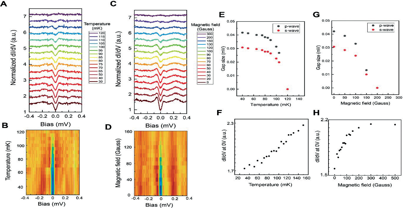
Figure. Temperature and magnetic-field evolution of the superconducting gap.(A,B) Normalized dI/dV spectra acquired at mK temperatures as a function of temperature, showing progressive filling of the superconducting gap and the inward shift of the coherence-like shoulders. (C,D) Normalized dI/dV spectra acquired at base temperature as a function of out-of-plane magnetic field, B || z, showing continuous suppression of the gap. (E) Gap magnitude extracted from fits to the temperature-dependent spectra, compared between isotropic s-wave and nodal-gap models. (G) Gap magnitude extracted from fits to the field-dependent spectra, again compared between isotropic s-wave and nodal-gap models. (E and G) Color maps of dI/dV as a function of bias and (E) temperature or (G) magnetic field, emphasizing the evolution of low-energy spectral weight through the superconducting phase diagram. (F and H) Zero-bias conductance as a function of (F) temperature and (H) magnetic field.The substantial and nearly linear increase of the zero-bias conductance with temperature, together with its rapid growth under field, is consistent with a soft low-energy excitation spectrum expected for nodal or near-nodal superconductivity.
As of 2025, the Dilution Refrigerator STM in CALDES is fully operational, and we started ultra-high-resolution Spectroscopic Imaging measurements on unconventional superconductors with extremely low Tc at millikelvin temperatures. Td-MoTe2 is a noncentrosymmetric type-II Weyl semimetal in which broken inversion symmetry produces spin-polarized bands, while its superconductivity emerges below 100 mK with the gap in the sub-mV range, rendering a direct determination of its pairing nature challenging. Using dilution-refrigerator spectroscopic-imaging scanning tunneling microscopy (SI-STM), we resolve the intrinsic superconducting gap of pristine Td-MoTe2 for the first time and trace its evolution with temperature and out-of-plane magnetic field. The results show a V-shaped gap of about 56 μeV, linear zero-bias conductance (ZBC) versus temperature, and field-induced ZBC increasing as √H. Remarkably, we observe particle-hole-symmetric in-gap quasiparticle-interference pattern (QPI) whose dispersion crosses at the exact zero bias unlike above Hc. Supported by model comparisons, our results identify a non-accidental nodal superconducting gap structure as well as the location of the nodes. (In preparation) We now focus on how such intrinsic nodal superconductivity emerges from the inversion-broken, spin-polarized, topologically non-trivial electronic structure of a Weyl semimetal
 Center for Artificial Low
Dimensional Electronic Systems
IBS POSTECH Campus 79, Jigok-ro 127beon-gil, Namgu, Pohang, Korea, (37673)
Tel+ 82-54-260-9022
Copyright(c) Center for Artificial Low Dimensional Electronic Systems at IBS.All Rights Reserved.