Research Program
Transport team
Discovery of new materials with desirable functionalities deepens our understanding on quantum nature of electronic degrees of freedom and their unconventional behaviors. The recent development of quantum materials and their fascinating transport phenomena showing the giant electromagnetic responses and also the hidden electronic phases beyond the conventional symmetry breaking orders. The CALDES-Transport Group, led by Prof. Jun Sung Kim, has focused on “Novel transport properties of designed topological and correlated low-dimensional materials under extreme conditions”. Our group are interested in both high-quality single crystal growth of quantum materials and their charge or spin transport under low temperatures, high magnetic fields and high pressures. Below are the brief summaries on our recent research, including some representative works.
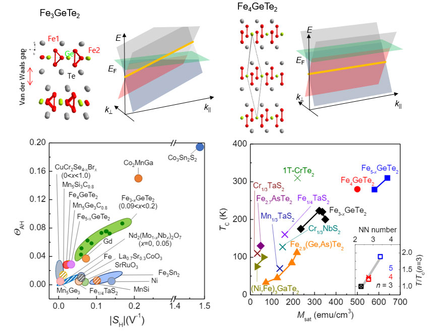
1. Giant electromagnetic responses of topological magnets.Recent remarkable discovery of graphene and topological insulators added another principle of quantum matter based on topological distinctions. Unlike ordinary quantum phases of matter, topological phases are not determined by a local order associated with broken symmetry but rather by a topological ingredient reflecting “twist” of electronic wave functions. In the course of exploring new low-dimensional materials with intriguing topological properties, we focused on magnetic materials, in which the interplay of magnetism and band topology can generate giant topological transport phenomena, potentially important for spin-related electronic applications. We firstly identified the topological nodal-line structure in a van der Waals (vdW) ferromagnet Fe3GeTe2 and presence of strong Berry curvature. As a result, a strong anomalous Hall effect is observed, which is much larger in strength than conventional ferromangets and robust against disorders [Nat. Mater. 2018]. This work led us to discover another vdW ferromagnet Fe4GeTe2, using computation material search and high quality single crystal growth, which exhibits nearly room temperature ferromagnetism and flat topological nodal-line structure [Sci. Adv. 2020]. Furthermore, we have succeeded to tune the interlayer magnetic interaction with chemical doping and thickness control in Fe4GeTe2, and induced a high-temperature antiferromagnetic phase in (Fe,Co)4GeTe2 [Nat. Commun. 2021, accepted]. Our series of discoveries on new topological van der Waals semimetals would provide a material platform to investigate the rich topological structures of low dimensional magnets and their functionalities for next-generation topological electronics or spintronics.
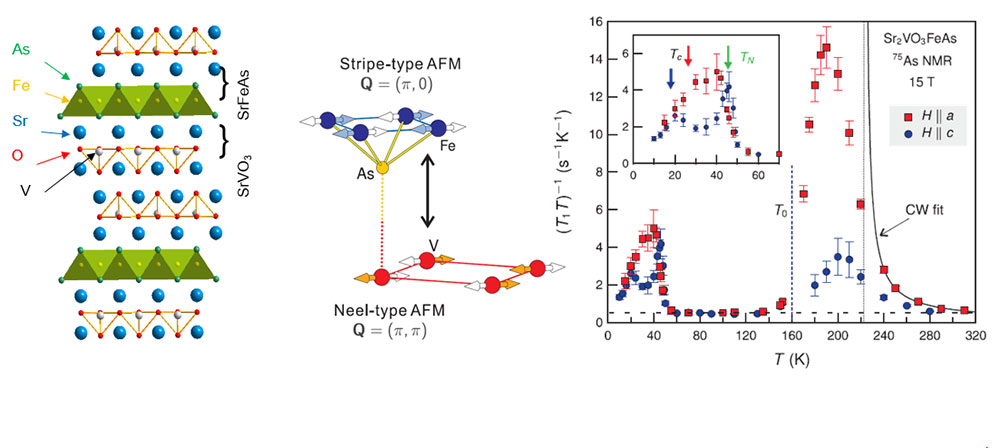
One of the central interests of our center is the interplay of distinct symmetries, topologies, and interaction as realized in the proximity field of artificial heterointerfaces. In the itinerant correlated electron systems such as iron-based superconductors (FeSCs), various types of Fermi surface instabilities are often frustrated, leading complex magnetic phases with broken time-reversal or lattice symmetries. Particularly, when the proximity-coupled layer is strongly correlated and magnetically active, the additional interfacial spin interaction may induce distinct ground states in FeSCs that has not been identified so far. As a model system, we have focused on a heterostructured FeSC, Sr2VO3FeAs as a model system, consisting of a FeSC layer and a Mott-insulating vanadium oxide layer. We find that an unusual charge/orbital order in the iron pnictide layers, without either static magnetism or broken C4-symmetry while suppressing the Neel antiferromagnetism in the vanadium oxide layers [Nat. Commun. 2017]. Such an unprecedented C4-symmetric hidden order is due to the frustration of the otherwise dominant iron stripe and vanadium Neel fluctuations via interfacial magnetic proximity coupling [ArXiv 2021], which also induces various unusual properties such as band-selective pseudogap [Phys. Rev. B. 2015, ArXiv 2020] or magnetically switchable superconductivities [Phys. Rev. Lett. 2017]. Our findings, therefore, manifest that the physics of itinerant correlated magnetic system can become even richer in the proximity of other correlated systems and also offer a new avenue for exploring unusual ground state in the correlated heterostructures.
 Center for Artificial Low
Dimensional Electronic Systems
IBS POSTECH Campus 79, Jigok-ro 127beon-gil, Namgu, Pohang, Korea, (37673)
Tel+ 82-54-260-9022
Copyright(c) Center for Artificial Low Dimensional Electronic Systems at IBS.All Rights Reserved.